Steward
分享是一種喜悅、更是一種幸福
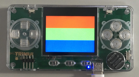
掌機 - TRIMUI - Assembly - LCD(TCON)
參考資料:
http://nano.lichee.pro/
https://mangopi.org/mangopi_r
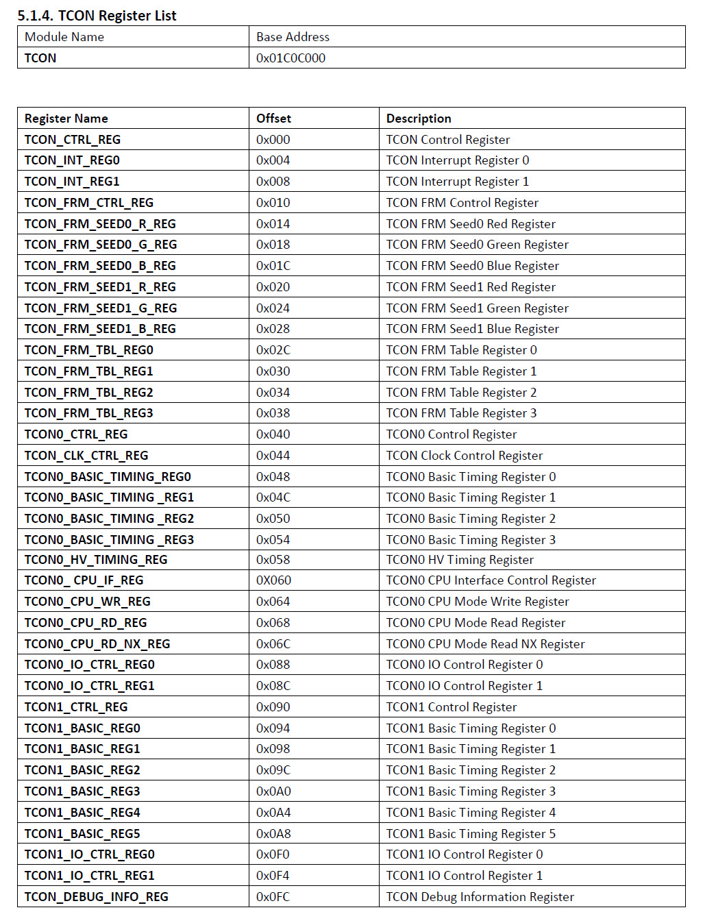
TCON
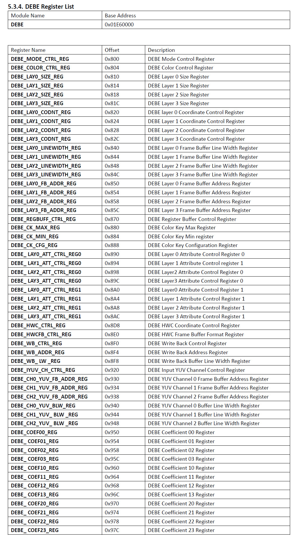
DEBE
main.s
    .global _start

    .equiv TCON_BASE,             0x01c0c000
    .equiv DRAM_BASE,             0x01c01000
    .equiv CCU_BASE,              0x01c20000
    .equiv GPIO_BASE,             0x01c20800
    .equiv UART1_BASE,            0x01c25400
    .equiv DEBE_BASE,             0x01e60000

    .equiv PLL_VIDEO_CTRL_REG,    0x0010
    .equiv PLL_DDR_CTRL_REG,      0x0020
    .equiv PLL_PERIPH_CTRL_REG,   0x0028
    .equiv AHB_APB_HCLKC_CFG_REG, 0x0054
    .equiv BUS_CLK_GATING_REG0,   0x0060
    .equiv BUS_CLK_GATING_REG1,   0x0064
    .equiv BUS_CLK_GATING_REG2,   0x0068
    .equiv DRAM_GATING_REG,       0x0100
    .equiv BUS_SOFT_RST_REG0,     0x02c0
    .equiv BUS_SOFT_RST_REG1,     0x02c4
    .equiv BUS_SOFT_RST_REG2,     0x02d0
    .equiv BE_CLK_REG,            0x0104
    .equiv FE_CLK_REG,            0x010C
    .equiv TCON_CLK_REG,          0x0118

    .equiv PA,                    (0x24 * 0)
    .equiv PB,                    (0x24 * 1)
    .equiv PC,                    (0x24 * 2)
    .equiv PD,                    (0x24 * 3)
    .equiv PE,                    (0x24 * 4)
    .equiv PF,                    (0x24 * 5)
    .equiv PORT_CFG0,             0x0000
    .equiv PORT_CFG1,             0x0004
    .equiv PORT_CFG2,             0x0008
    .equiv PORT_DATA,             0x0010
    .equiv SDR_PAD_DRV,           0x02c0
    .equiv SDR_PAD_PUL,           0x02c4

    .equiv UART_RBR,              0x0000
    .equiv UART_DLL,              0x0000
    .equiv UART_DLH,              0x0004
    .equiv UART_IER,              0x0004
    .equiv UART_IIR,              0x0008
    .equiv UART_LCR,              0x000c
    .equiv UART_MCR,              0x0010
    .equiv UART_USR,              0x007c

    .equiv DRAM_SCONR,            0x00
    .equiv DRAM_STMG0R,           0x04
    .equiv DRAM_STMG1R,           0x08
    .equiv DRAM_SCTLR,            0x0c
    .equiv DRAM_SREFR,            0x10
    .equiv DRAM_DDLYR,            0x24
    .equiv DRAM_DRPTR0,           0x30

    .equiv TCON_CTRL_REG,           0x000
    .equiv TCON_INT_REG0,           0x004
    .equiv TCON_INT_REG1,           0x008
    .equiv TCON_FRM_CTRL_REG,       0x010
    .equiv TCON_FRM_SEED0_R_REG,    0x014
    .equiv TCON_FRM_SEED0_G_REG,    0x018
    .equiv TCON_FRM_SEED0_B_REG,    0x01C
    .equiv TCON_FRM_SEED1_R_REG,    0x020
    .equiv TCON_FRM_SEED1_G_REG,    0x024
    .equiv TCON_FRM_SEED1_B_REG,    0x028
    .equiv TCON_FRM_TBL_REG0,       0x02C
    .equiv TCON_FRM_TBL_REG1,       0x030
    .equiv TCON_FRM_TBL_REG2,       0x034
    .equiv TCON_FRM_TBL_REG3,       0x038
    .equiv TCON0_CTRL_REG,          0x040
    .equiv TCON_CLK_CTRL_REG,       0x044
    .equiv TCON0_BASIC_TIMING_REG0, 0x048
    .equiv TCON0_BASIC_TIMING_REG1, 0x04C
    .equiv TCON0_BASIC_TIMING_REG2, 0x050
    .equiv TCON0_BASIC_TIMING_REG3, 0x054
    .equiv TCON0_HV_TIMING_REG,     0x058
    .equiv TCON0_CPU_IF_REG,        0x060
    .equiv TCON0_CPU_WR_REG,        0x064
    .equiv TCON0_CPU_RD_REG,        0x068
    .equiv TCON0_CPU_RD_NX_REG,     0x06C
    .equiv TCON0_IO_CTRL_REG0,      0x088
    .equiv TCON0_IO_CTRL_REG1,      0x08C
    .equiv TCON1_CTRL_REG,          0x090
    .equiv TCON1_BASIC_REG0,        0x094
    .equiv TCON1_BASIC_REG1,        0x098
    .equiv TCON1_BASIC_REG2,        0x09C
    .equiv TCON1_BASIC_REG3,        0x0A0
    .equiv TCON1_BASIC_REG4,        0x0A4
    .equiv TCON1_BASIC_REG5,        0x0A8
    .equiv TCON1_IO_CTRL_REG0,      0x0F0
    .equiv TCON1_IO_CTRL_REG1,      0x0F4
    .equiv TCON_DEBUG_INFO_REG,     0x0FC

    .equiv DEBE_MODE_CTRL_REG,       0x800
    .equiv DEBE_COLOR_CTRL_REG,      0x804
    .equiv DEBE_DISP_SIZE_REG,       0x808
    .equiv DEBE_LAY0_SIZE_REG,       0x810
    .equiv DEBE_LAY1_SIZE_REG,       0x814
    .equiv DEBE_LAY2_SIZE_REG,       0x818
    .equiv DEBE_LAY3_SIZE_REG,       0x81C
    .equiv DEBE_LAY0_CODNT_REG,      0x820
    .equiv DEBE_LAY1_CODNT_REG,      0x824
    .equiv DEBE_LAY2_CODNT_REG,      0x828
    .equiv DEBE_LAY3_CODNT_REG,      0x82C
    .equiv DEBE_LAY0_LINEWIDTH_REG,  0x840
    .equiv DEBE_LAY1_LINEWIDTH_REG,  0x844
    .equiv DEBE_LAY2_LINEWIDTH_REG,  0x848
    .equiv DEBE_LAY3_LINEWIDTH_REG,  0x84C
    .equiv DEBE_LAY0_FB_ADDR_REG,    0x850
    .equiv DEBE_LAY1_FB_ADDR_REG,    0x854
    .equiv DEBE_LAY2_FB_ADDR_REG,    0x858
    .equiv DEBE_LAY3_FB_ADDR_REG,    0x85C
    .equiv DEBE_LAY0_FB_HI_ADDR_REG, 0x860
    .equiv DEBE_LAY1_FB_HI_ADDR_REG, 0x864
    .equiv DEBE_LAY2_FB_HI_ADDR_REG, 0x868
    .equiv DEBE_LAY3_FB_HI_ADDR_REG, 0x86c
    .equiv DEBE_REGBUFF_CTRL_REG,    0x870
    .equiv DEBE_LAY0_ATT_CTRL_REG0,  0x890
    .equiv DEBE_LAY1_ATT_CTRL_REG0,  0x894
    .equiv DEBE_LAY2_ATT_CTRL_REG0,  0x898
    .equiv DEBE_LAY3_ATT_CTRL_REG0,  0x89C
    .equiv DEBE_LAY0_ATT_CTRL_REG1,  0x8A0
    .equiv DEBE_LAY1_ATT_CTRL_REG1,  0x8A4
    .equiv DEBE_LAY2_ATT_CTRL_REG1,  0x8A8
    .equiv DEBE_LAY3_ATT_CTRL_REG1,  0x8AC

    .equiv XRES,          320
    .equiv YRES,          240
    .equiv V_FRONT_PORCH, 0x11e
    .equiv V_BACK_PORCH,  2
    .equiv V_SYNC_LEN,    1
    .equiv H_SYNC_LEN,    0x12
    .equiv H_BACK_PORCH,  2
    .equiv H_FRONT_PORCH, 0x465
    .equiv VRAM_PHYS,     0x80000000

    .arm
    .text
_start:
    .long 0xea000016
    .byte 'e', 'G', 'O', 'N', '.', 'B', 'T', '0'
    .long 0, __spl_size
    .byte 'S', 'P', 'L', 2
    .long 0, 0
    .long 0, 0, 0, 0, 0, 0, 0, 0
    .long 0, 0, 0, 0, 0, 0, 0, 0

_vector:
    b reset
    b .
    b .
    b .
    b .
    b .
    b .
    b .

reset:
    mov sp, #0x8000
    bl init_pll_module
    bl init_uart_module
    bl init_dram_module

    ldr r1, =VRAM_PHYS
    ldr r2, =XRES * 80 * 2
    ldr r3, =0xf800f800
0:
    str r3, [r1]
    add r1, #4
    subs r2, #4
    bne 0b

    ldr r2, =XRES * 80 * 2
    ldr r3, =0x07e007e0
0:
    str r3, [r1]
    add r1, #4
    subs r2, #4
    bne 0b

    ldr r2, =XRES * 80 * 2
    ldr r3, =0x001f001f
0:
    str r3, [r1]
    add r1, #4
    subs r2, #4
    bne 0b

    bl init_tcon_module
    b .

spi_9bits_write:
    push {r4, lr}
    ldr r4, =GPIO_BASE
    ldr r2, [r4, #(PD + PORT_DATA)]
    bic r2, #(1 << 11)
    str r2, [r4, #(PD + PORT_DATA)]

    ldr r1, =9
0:
    tst r0, #0x100
    biceq r2, #(1 << 10)
    orrne r2, #(1 << 10)
    lsl r0, #1

    bic r2, #(1 << 9)
    str r2, [r4, #(PD + PORT_DATA)]
    orr r2, #(1 << 9)
    str r2, [r4, #(PD + PORT_DATA)]

    subs r1, #1
    bne 0b

    orr r2, #(1 << 11)
    str r2, [r4, #(PD + PORT_DATA)]
    pop {r4, pc}

init_lcd_module:
    push {lr}
    ldr r0, =0x00fe
    bl spi_9bits_write
    ldr r0, =0x00ef
    bl spi_9bits_write
    ldr r0, =0x0036
    bl spi_9bits_write
    ldr r0, =0x0140
    bl spi_9bits_write
    ldr r0, =0x003a
    bl spi_9bits_write
    ldr r0, =0x0155
    bl spi_9bits_write
    ldr r0, =0x0084
    bl spi_9bits_write
    ldr r0, =0x0104
    bl spi_9bits_write
    ldr r0, =0x0086
    bl spi_9bits_write
    ldr r0, =0x01fb
    bl spi_9bits_write
    ldr r0, =0x0087
    bl spi_9bits_write
    ldr r0, =0x0179
    bl spi_9bits_write
    ldr r0, =0x0089
    bl spi_9bits_write
    ldr r0, =0x010b
    bl spi_9bits_write
    ldr r0, =0x008a
    bl spi_9bits_write
    ldr r0, =0x0120
    bl spi_9bits_write
    ldr r0, =0x008b
    bl spi_9bits_write
    ldr r0, =0x0180
    bl spi_9bits_write
    ldr r0, =0x008d
    bl spi_9bits_write
    ldr r0, =0x013b
    bl spi_9bits_write
    ldr r0, =0x008e
    bl spi_9bits_write
    ldr r0, =0x01cf
    bl spi_9bits_write
    ldr r0, =0x00ec
    bl spi_9bits_write
    ldr r0, =0x0133
    bl spi_9bits_write
    ldr r0, =0x0102
    bl spi_9bits_write
    ldr r0, =0x014c
    bl spi_9bits_write
    ldr r0, =0x0098
    bl spi_9bits_write
    ldr r0, =0x013e
    bl spi_9bits_write
    ldr r0, =0x009c
    bl spi_9bits_write
    ldr r0, =0x014b
    bl spi_9bits_write
    ldr r0, =0x0099
    bl spi_9bits_write
    ldr r0, =0x013e
    bl spi_9bits_write
    ldr r0, =0x009d
    bl spi_9bits_write
    ldr r0, =0x014b
    bl spi_9bits_write
    ldr r0, =0x009b
    bl spi_9bits_write
    ldr r0, =0x0155
    bl spi_9bits_write
    ldr r0, =0x00e8
    bl spi_9bits_write
    ldr r0, =0x0111
    bl spi_9bits_write
    ldr r0, =0x0100
    bl spi_9bits_write
    ldr r0, =0x00ff
    bl spi_9bits_write
    ldr r0, =0x0162
    bl spi_9bits_write
    ldr r0, =0x00c3
    bl spi_9bits_write
    ldr r0, =0x0120
    bl spi_9bits_write
    ldr r0, =0x00c4
    bl spi_9bits_write
    ldr r0, =0x0103
    bl spi_9bits_write
    ldr r0, =0x00c9
    bl spi_9bits_write
    ldr r0, =0x010a
    bl spi_9bits_write
    ldr r0, =0x003a
    bl spi_9bits_write
    ldr r0, =0x0155
    bl spi_9bits_write
    ldr r0, =0x0084
    bl spi_9bits_write
    ldr r0, =0x0161
    bl spi_9bits_write
    ldr r0, =0x008a
    bl spi_9bits_write
    ldr r0, =0x0140
    bl spi_9bits_write
    ldr r0, =0x00f6
    bl spi_9bits_write
    ldr r0, =0x01c7
    bl spi_9bits_write
    ldr r0, =0x00b0
    bl spi_9bits_write
    ldr r0, =0x0163
    bl spi_9bits_write
    ldr r0, =0x00b5
    bl spi_9bits_write
    ldr r0, =0x0102
    bl spi_9bits_write
    ldr r0, =0x0102
    bl spi_9bits_write
    ldr r0, =0x0114
    bl spi_9bits_write
    ldr r0, =0x00f0
    bl spi_9bits_write
    ldr r0, =0x014a
    bl spi_9bits_write
    ldr r0, =0x0110
    bl spi_9bits_write
    ldr r0, =0x010a
    bl spi_9bits_write
    ldr r0, =0x010a
    bl spi_9bits_write
    ldr r0, =0x0126
    bl spi_9bits_write
    ldr r0, =0x0139
    bl spi_9bits_write
    ldr r0, =0x00f2
    bl spi_9bits_write
    ldr r0, =0x014a
    bl spi_9bits_write
    ldr r0, =0x0110
    bl spi_9bits_write
    ldr r0, =0x010a
    bl spi_9bits_write
    ldr r0, =0x010a
    bl spi_9bits_write
    ldr r0, =0x0126
    bl spi_9bits_write
    ldr r0, =0x0139
    bl spi_9bits_write
    ldr r0, =0x00f1
    bl spi_9bits_write
    ldr r0, =0x0150
    bl spi_9bits_write
    ldr r0, =0x018f
    bl spi_9bits_write
    ldr r0, =0x01af
    bl spi_9bits_write
    ldr r0, =0x013b
    bl spi_9bits_write
    ldr r0, =0x013f
    bl spi_9bits_write
    ldr r0, =0x017f
    bl spi_9bits_write
    ldr r0, =0x00f3
    bl spi_9bits_write
    ldr r0, =0x0150
    bl spi_9bits_write
    ldr r0, =0x018f
    bl spi_9bits_write
    ldr r0, =0x01af
    bl spi_9bits_write
    ldr r0, =0x013b
    bl spi_9bits_write
    ldr r0, =0x013f
    bl spi_9bits_write
    ldr r0, =0x017f
    bl spi_9bits_write
    ldr r0, =0x00ba
    bl spi_9bits_write
    ldr r0, =0x010a
    bl spi_9bits_write
    ldr r0, =0x0035
    bl spi_9bits_write
    ldr r0, =0x0100
    bl spi_9bits_write
    ldr r0, =0x0021
    bl spi_9bits_write
    ldr r0, =0x00fe
    bl spi_9bits_write
    ldr r0, =0x00ee
    bl spi_9bits_write
    ldr r0, =0x0011
    bl spi_9bits_write
    ldr r0, =0x0029
    bl spi_9bits_write
    ldr r0, =0x002c
    bl spi_9bits_write
    pop {pc}

init_tcon_module:
    push {r4, lr}
    ldr r4, =GPIO_BASE
    ldr r1, [r4, #(PD + PORT_CFG0)]
    ldr r2, =0xfffff000
    bic r1, r2
    ldr r2, =0x22222000
    orr r1, r2
    str r1, [r4, #(PD + PORT_CFG0)]

    ldr r1, [r4, #(PD + PORT_CFG1)]
    ldr r2, =0x0000ffff
    bic r1, r2
    ldr r2, =0x00001112
    orr r1, r2
    str r1, [r4, #(PD + PORT_CFG1)]

    ldr r1, [r4, #(PD + PORT_CFG2)]
    ldr r2, =0x00ff0f00
    bic r1, r2
    ldr r2, =0x00220200
    orr r1, r2
    str r1, [r4, #(PD + PORT_CFG2)]

    ldr r1, [r4, #(PE + PORT_CFG0)]
    ldr r2, =0x0f000000
    bic r1, r2
    ldr r2, =0x01000000
    orr r1, r2
    str r1, [r4, #(PE + PORT_CFG0)]

    ldr r1, =0xffffffff
    str r1, [r4, #(PD + PORT_DATA)]

    ldr r1, =0xffffffff
    str r1, [r4, #(PE + PORT_DATA)]

    bl init_lcd_module

    ldr r4, =CCU_BASE
    ldr r1, =(1 << 31) | (1 << 25) | (1 << 24) | (98 << 8) | (7 << 0)
    str r1, [r4, #PLL_VIDEO_CTRL_REG]

    ldr r1, [r4, #DRAM_GATING_REG]
    orr r1, #(1 << 26) | (1 << 24)
    str r1, [r4, #DRAM_GATING_REG]

    ldr r1, [r4, #FE_CLK_REG]
    orr r1, #(1 << 31)
    str r1, [r4, #FE_CLK_REG]

    ldr r1, [r4, #BE_CLK_REG]
    orr r1, #(1 << 31)
    str r1, [r4, #BE_CLK_REG]

    ldr r1, [r4, #TCON_CLK_REG]
    orr r1, #(1 << 31)
    orr r1, #(1 << 25)
    str r1, [r4, #TCON_CLK_REG]

    ldr r1, [r4, #BUS_CLK_GATING_REG1]
    orr r1, #(1 << 14)
    orr r1, #(1 << 12)
    orr r1, #(1 << 4)
    str r1, [r4, #BUS_CLK_GATING_REG1]

    ldr r1, [r4, #BUS_SOFT_RST_REG1]
    orr r1, #(1 << 14)
    orr r1, #(1 << 12)
    orr r1, #(1 << 4)
    str r1, [r4, #BUS_SOFT_RST_REG1]

    ldr r1, =DEBE_BASE + 0x800
    ldr r2, =0x200
    ldr r3, =0
0:
    str r3, [r1]
    add r1, #4
    subs r2, #4
    bne 0b

    ldr r4, =TCON_BASE
    ldr r1, [r4, #TCON_CTRL_REG]
    bic r1, #(1 << 0)
    str r1, [r4, #TCON_CTRL_REG]

    ldr r4, =DEBE_BASE
    ldr r1, [r4, #DEBE_MODE_CTRL_REG]
    orr r1, #(1 << 0)
    str r1, [r4, #DEBE_MODE_CTRL_REG]

    ldr r1, =(XRES << 4)
    str r1, [r4, #DEBE_LAY0_LINEWIDTH_REG]

    ldr r1, =(5 << 8)
    str r1, [r4, #DEBE_LAY0_ATT_CTRL_REG1]

    ldr r1, =((YRES - 1) << 16) | ((XRES - 1) << 0)
    str r1, [r4, #DEBE_DISP_SIZE_REG]
    str r1, [r4, #DEBE_LAY0_SIZE_REG]

    ldr r1, [r4, #DEBE_MODE_CTRL_REG]
    orr r1, #(1 << 8)
    str r1, [r4, #DEBE_MODE_CTRL_REG]

    ldr r1, [r4, #DEBE_REGBUFF_CTRL_REG]
    orr r1, #(1 << 0)
    str r1, [r4, #DEBE_REGBUFF_CTRL_REG]

    ldr r1, [r4, #DEBE_MODE_CTRL_REG]
    orr r1, #(1 << 1)
    str r1, [r4, #DEBE_MODE_CTRL_REG]

    ldr r1, =VRAM_PHYS << 3
    str r1, [r4, #DEBE_LAY0_FB_ADDR_REG]

    ldr r1, =VRAM_PHYS >> 29
    str r1, [r4, #DEBE_LAY0_FB_HI_ADDR_REG]

    ldr r4, =TCON_BASE
    ldr r1, =(1 << 31) | (((V_FRONT_PORCH + V_BACK_PORCH + V_SYNC_LEN) & 0x1f) << 4)
    str r1, [r4, #TCON0_CTRL_REG]

    ldr r1, =(0xf << 28) | (25 << 0)
    str r1, [r4, #TCON_CLK_CTRL_REG]

    ldr r1, =(YRES - 1) << 0
    ldr r2, =(XRES - 1) << 16
    orr r1, r2
    str r1, [r4, #TCON0_BASIC_TIMING_REG0]

    ldr r1, =((H_SYNC_LEN + H_BACK_PORCH) - 1) << 0
    ldr r2, =((XRES + H_FRONT_PORCH + H_SYNC_LEN + H_BACK_PORCH) - 1) << 16
    orr r1, r2
    str r1, [r4, #TCON0_BASIC_TIMING_REG1]

    ldr r1, =((V_SYNC_LEN + V_BACK_PORCH) - 1) << 0
    ldr r2, =((YRES + V_FRONT_PORCH + V_SYNC_LEN + V_BACK_PORCH) - 1) << 16
    orr r1, r2
    str r1, [r4, #TCON0_BASIC_TIMING_REG2]

    ldr r1, =(V_SYNC_LEN - 1) << 0
    ldr r2, =(H_SYNC_LEN - 1) << 16
    orr r1, r2
    str r1, [r4, #TCON0_BASIC_TIMING_REG3]

    ldr r1, =0
    str r1, [r4, #TCON0_CPU_IF_REG]

    ldr r1, =(1 << 31)
    str r1, [r4, #TCON0_HV_TIMING_REG]

    ldr r1, =0x11111111
    str r1, [r4, #TCON_FRM_SEED0_R_REG]
    str r1, [r4, #TCON_FRM_SEED0_G_REG]
    str r1, [r4, #TCON_FRM_SEED0_B_REG]
    str r1, [r4, #TCON_FRM_SEED1_R_REG]
    str r1, [r4, #TCON_FRM_SEED1_G_REG]
    str r1, [r4, #TCON_FRM_SEED1_B_REG]

    ldr r1, =0x01010000
    str r1, [r4, #TCON_FRM_TBL_REG0]
    ldr r1, =0x15151111
    str r1, [r4, #TCON_FRM_TBL_REG1]
    ldr r1, =0x57575555
    str r1, [r4, #TCON_FRM_TBL_REG2]
    ldr r1, =0x7f7f7777
    str r1, [r4, #TCON_FRM_TBL_REG3]

    ldr r1, =(1 << 31) | (5 << 4)
    str r1, [r4, #TCON_FRM_CTRL_REG]

    ldr r1, =(1 << 28) | (1 << 25) | (1 << 24)
    str r1, [r4, #TCON0_IO_CTRL_REG0]

    ldr r1, =0
    str r1, [r4, #TCON0_IO_CTRL_REG1]

    ldr r1, =0
    str r1, [r4, #TCON_INT_REG0]

    ldr r1, [r4, #TCON_CTRL_REG]
    orr r1, #(1 << 31)
    str r1, [r4, #TCON_CTRL_REG]
    pop {r4, pc}

init_pll_module:
    push {r4, lr}
    ldr r4, =CCU_BASE

    ldr r1, =0x80041800
    str r1, [r4, #PLL_PERIPH_CTRL_REG]

    ldr r1, =0x00003180
    str r1, [r4, #AHB_APB_HCLKC_CFG_REG]
    pop {r4, pc}

init_uart_module:
    push {r4, lr}
    ldr r4, =GPIO_BASE

    ldr r1, [r4, #(PA + PORT_CFG0)]
    bic r1, #0xff00
    orr r1, #0x5500
    str r1, [r4, #(PA + PORT_CFG0)]

    ldr r4, =CCU_BASE
    ldr r1, [r4, #BUS_CLK_GATING_REG2]
    orr r1, #(1 << 21)
    str r1, [r4, #BUS_CLK_GATING_REG2]

    ldr r1, [r4, #BUS_SOFT_RST_REG2]
    orr r1, #(1 << 21)
    str r1, [r4, #BUS_SOFT_RST_REG2]

    ldr r4, =UART1_BASE
    mov r1, #0x00
    str r1, [r4, #UART_IER]
    mov r1, #0xf7
    str r1, [r4, #UART_IIR]
    mov r1, #0x00
    str r1, [r4, #UART_MCR]
    ldr r1, [r4, #UART_LCR]
    orr r1, #(1 << 7)
    str r1, [r4, #UART_LCR]
    mov r1, #54
    str r1, [r4, #UART_DLL]
    mov r1, #0x00
    str r1, [r4, #UART_DLH]
    ldr r1, [r4, #UART_LCR]
    bic r1, #(1 << 7)
    str r1, [r4, #UART_LCR]
    ldr r1, [r4, #UART_LCR]
    bic r1, #0x1f
    orr r1, #0x03
    str r1, [r4, #UART_LCR]
    pop {r4, pc}

uart_send_byte:
    push {r4, lr}
    ldr r4, =UART1_BASE
1:
    ldr r1, [r4, #UART_USR]
    tst r1, #(1 << 1)
    beq 1b
    strb r0, [r4, #UART_RBR]
    pop {r4, pc}

uart_send_4byte:
    push {r4, lr}
    mov r4, r0
    lsr r0, #24
    bl uart_send_byte
    mov r0, r4
    lsr r0, #16
    bl uart_send_byte
    mov r0, r4
    lsr r0, #8
    bl uart_send_byte
    mov r0, r4
    bl uart_send_byte
    pop {r4, pc}

sdelay:
    push {lr}
0:
    subs r0, #1
    bne 0b
    pop {pc}

dram_delay:
    push {lr}
    ldr r1, =2000
    mul r0, r1
    bl sdelay
    pop {pc}

dram_delay_scan:
    push {r4, lr}
    ldr r4, =DRAM_BASE
    ldr r1, [r4, #DRAM_DDLYR]
    orr r1, #1
    str r1, [r4, #DRAM_DDLYR]
0:
    ldr r1, [r4, #DRAM_DDLYR]
    tst r1, #1
    bne 0b
    pop {r4, pc}

dram_para_setup:
    push {r4, lr}
    ldr r4, =DRAM_BASE
    ldr r1, =0x1200a
    ldr r2, =dram_row
    ldr r2, [r2]
    sub r2, #1
    lsl r2, #5
    orr r1, r2
    ldr r2, =dram_col
    ldr r2, [r2]
    sub r2, #1
    lsl r2, #9
    orr r1, r2
    str r1, [r4, #DRAM_SCONR]

    ldr r1, [r4, #DRAM_SCTLR]
    orr r1, #(1 << 19)
    str r1, [r4, #DRAM_SCTLR]

    ldr r1, [r4, #DRAM_SCTLR]
    orr r1, #1
    str r1, [r4, #DRAM_SCTLR]
0:
    ldr r1, [r4, #DRAM_SCTLR]
    tst r1, #1
    bne 0b
    pop {r4, pc}

dram_scan_readpipe:
    push {r4, r5, lr}
    ldr r4, =DRAM_BASE
    mov r5, #0
0:
    ldr r1, [r4, #DRAM_SCTLR]
    bic r1, #(7 << 6)
    orr r1, r5, lsl #6
    str r1, [r4, #DRAM_SCTLR]

    bl dram_delay_scan

    ldr r1, [r4, #DRAM_DDLYR]
    lsr r1, #4
    ands r1, #3
    beq 1f

    add r5, #1
    cmp r5, #8
    bcc 0b

1:
    ldr r1, [r4, #DRAM_SCTLR]
    bic r1, #(7 << 6)
    orr r1, r5, lsl #6
    str r1, [r4, #DRAM_SCTLR]

    bl dram_delay_scan
    pop {r4, r5, pc}

dram_get_dram_size:
    push {r4, r5, r6, lr}
    ldr r4, =DRAM_BASE

    ldr r1, =dram_col
    ldr r2, =10
    str r2, [r1]

    ldr r1, =dram_row
    ldr r2, =13
    str r2, [r1]

    bl dram_para_setup
    bl dram_scan_readpipe

    mov r1, #0
    ldr r2, =0x80000200
    ldr r3, =0x80000600
    ldr r4, =0x11111111
    ldr r5, =0x22222222
0:
    add r2, r1
    str r4, [r2]
    add r3, r1
    str r5, [r3]
    add r1, #1
    cmp r1, #32
    bcc 0b

    mov r1, #0
    ldr r2, =0x80000200
    mov r4, #0
0:
    add r2, r1
    ldr r3, [r2]
    cmp r3, r5
    addeq r4, #1
    add r1, #1
    cmp r1, #32
    bcc 0b

    cmp r4, #32
    moveq r5, #9
    movne r5, #10
    ldr r2, =dram_col
    str r5, [r2]

    bl dram_para_setup

    cmp r5, #10
    ldreq r1, =0x80400000
    ldreq r2, =0x80c00000
    ldrne r1, =0x80200000
    ldrne r2, =0x80600000
    ldr r3, =0x33333333
    ldr r4, =0x44444444
    mov r6, r1
    mov r0, #0
0:
    add r1, r0
    str r3, [r1]
    add r2, r0
    str r4, [r2]
    add r0, #1
    cmp r0, #32
    bcc 0b

    mov r0, #0
    mov r1, #0
    mov r2, r6
0:
    add r2, r1
    ldr r3, [r2]
    cmp r3, r4
    addeq r0, #1
    add r1, #1
    cmp r1, #32
    bcc 0b

    cmp r0, #32
    moveq r1, #12
    movne r1, #13
    ldr r2, =dram_row
    str r1, [r2]

    ldr r1, =dram_row
    ldr r1, [r1]
    cmp r1, #13
    beq 0f
    mov r2, #16
    b 1f
0:
    ldr r1, =dram_col
    ldr r1, [r1]
    cmp r1, #10
    bne 0f
    mov r2, #64
    b 1f
0:
    mov r2, #32
1:
    ldr r1, =dram_size
    str r2, [r1]

    ldr r1, =(156 * 499) >> 6
    str r1, [r4, #DRAM_SREFR]
    bl dram_para_setup
    pop {r4, r5, r6, pc}

init_dram_module:
    push {r4, r5, r6, lr}
    ldr r4, =GPIO_BASE
    ldr r5, =CCU_BASE
    ldr r6, =DRAM_BASE
    ldr r1, [r4, #(PB + PORT_CFG0)]
    orr r1, #(7 << 12)
    str r1, [r4, #(PB + PORT_CFG0)]

    ldr r0, =5
    bl dram_delay

    ldr r1, =0xaaa
    str r1, [r4, #SDR_PAD_DRV]

    ldr r1, =(1 << 31) | (1 << 20) | (((156 * 2) / 24 - 1) << 8)
    str r1, [r5, #PLL_DDR_CTRL_REG]
0:
    ldr r1, [r5, #PLL_DDR_CTRL_REG]
    tst r1, #(1 << 28)
    beq 0b

    ldr r1, [r5, #BUS_CLK_GATING_REG0]
    orr r1, #(1 << 14)
    str r1, [r5, #BUS_CLK_GATING_REG0]

    ldr r1, [r5, #BUS_SOFT_RST_REG0]
    orr r1, #(1 << 14)
    str r1, [r5, #BUS_SOFT_RST_REG0]

    ldr r1, [r4, #SDR_PAD_PUL]
    orr r1, #(1 << 16)
    str r1, [r4, #SDR_PAD_PUL]

    ldr r1, =0xb7ceedc2
    str r1, [r6, #DRAM_STMG0R]

    ldr r1, =0xa70008
    str r1, [r6, #DRAM_STMG1R]

    bl dram_para_setup

    ldr r1, =(156 * 499) >> 6
    str r1, [r6, #DRAM_SREFR]

    bl dram_scan_readpipe
    bl dram_get_dram_size
    pop {r4, r5, r6, pc}

.data
    dram_size: .word 32
    dram_col:  .word 10
    dram_row:  .word 13
    .end
完成