Miyoo >> Assembly
DRAM
參考資料:
1. pdf
2. xboot
3. lichee
4. mangopi_r
5. allwinner
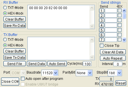
關於F1C100S DRAM的相關資料,司徒花了相當多時間尋找,可惜沒有找到相關的文件說明,唯一可以參考的程式碼就是XBoot的DRAM初始話程式碼
main.s
  .global _start

  .equiv DRAM_BASE,             0x01c01000
  .equiv CCU_BASE,              0x01c20000
  .equiv GPIO_BASE,             0x01c20800
  .equiv UART1_BASE,            0x01c25400

  .equiv PLL_DDR_CTRL_REG,      0x0020
  .equiv PLL_PERIPH_CTRL_REG,   0x0028
  .equiv AHB_APB_HCLKC_CFG_REG, 0x0054
  .equiv BUS_CLK_GATING_REG0,   0x0060
  .equiv BUS_CLK_GATING_REG2,   0x0068
  .equiv DRAM_GATING_REG,       0x0100
  .equiv BUS_SOFT_RST_REG0,     0x02c0
  .equiv BUS_SOFT_RST_REG2,     0x02d0

  .equiv PA,                    (0x24 * 0)
  .equiv PB,                    (0x24 * 1)
  .equiv PORT_CFG0,             0x0000
  .equiv PORT_DATA,             0x0010
  .equiv SDR_PAD_DRV,           0x02c0
  .equiv SDR_PAD_PUL,           0x02c4

  .equiv UART_RBR,              0x0000
  .equiv UART_DLL,              0x0000
  .equiv UART_DLH,              0x0004
  .equiv UART_IER,              0x0004
  .equiv UART_IIR,              0x0008
  .equiv UART_LCR,              0x000c
  .equiv UART_MCR,              0x0010
  .equiv UART_USR,              0x007c

  .equiv DRAM_SCONR,            0x00
  .equiv DRAM_STMG0R,           0x04
  .equiv DRAM_STMG1R,           0x08
  .equiv DRAM_SCTLR,            0x0c
  .equiv DRAM_SREFR,            0x10
  .equiv DRAM_DDLYR,            0x24
  .equiv DRAM_DRPTR0,           0x30

  .arm
  .text
_start:
  .long 0xea000016
  .byte 'e', 'G', 'O', 'N', '.', 'B', 'T', '0'
  .long 0, __spl_size
  .byte 'S', 'P', 'L', 2
  .long 0, 0
  .long 0, 0, 0, 0, 0, 0, 0, 0
  .long 0, 0, 0, 0, 0, 0, 0, 0

_vector:
  b reset
  b .
  b .
  b .
  b .
  b .
  b .
  b .

reset:
  bl init_pll_module
  bl init_uart_module
  bl init_dram_module

  ldr r1, =dram_size
  ldr r0, [r1]
  bl uart_send_4byte

  ldr r1, =dram_size
  ldr r1, [r1]
  cmp r1, #16
  ldreq r3, =(16 * 1024 * 1024) / 4
  cmp r1, #32
  ldreq r3, =(32 * 1024 * 1024) / 4
  cmp r1, #64
  ldreq r3, =(64 * 1024 * 1024) / 4

  ldr r5, =0x80000000
  mov r4, r5
  mov r1, #0
0:
  str r1, [r4]
  add r4, #4
  add r1, #1
  cmp r1, r3
  bcc 0b

  mov r4, r5
  mov r1, #0
1:
  ldr r2, [r4]
  cmp r2, r1
  bne 2f
  add r4, #4
  add r1, #1
  cmp r1, r3
  bcc 1b
2:
  mov r0, r4
  bl uart_send_4byte
  b .

init_pll_module:
  push {r4, lr}
  ldr r4, =CCU_BASE

  ldr r1, =0x80041800
  str r1, [r4, #PLL_PERIPH_CTRL_REG]

  ldr r1, =0x00003180
  str r1, [r4, #AHB_APB_HCLKC_CFG_REG]
  pop {r4, pc}

init_uart_module:
  push {r4, lr}
  ldr r4, =GPIO_BASE

  ldr r1, [r4, #(PA + PORT_CFG0)]
  bic r1, #0xff00
  orr r1, #0x5500
  str r1, [r4, #(PA + PORT_CFG0)]

  ldr r4, =CCU_BASE
  ldr r1, [r4, #BUS_CLK_GATING_REG2]
  orr r1, #(1 << 21)
  str r1, [r4, #BUS_CLK_GATING_REG2]

  ldr r1, [r4, #BUS_SOFT_RST_REG2]
  orr r1, #(1 << 21)
  str r1, [r4, #BUS_SOFT_RST_REG2]

  ldr r4, =UART1_BASE
  mov r1, #0x00
  str r1, [r4, #UART_IER]
  mov r1, #0xf7
  str r1, [r4, #UART_IIR]
  mov r1, #0x00
  str r1, [r4, #UART_MCR]
  ldr r1, [r4, #UART_LCR]
  orr r1, #(1 << 7)
  str r1, [r4, #UART_LCR]
  mov r1, #54
  str r1, [r4, #UART_DLL]
  mov r1, #0x00
  str r1, [r4, #UART_DLH]
  ldr r1, [r4, #UART_LCR]
  bic r1, #(1 << 7)
  str r1, [r4, #UART_LCR]
  ldr r1, [r4, #UART_LCR]
  bic r1, #0x1f
  orr r1, #0x03
  str r1, [r4, #UART_LCR]
  pop {r4, pc}

uart_send_byte:
  push {r4, lr}
  ldr r4, =UART1_BASE
1:
  ldr r1, [r4, #UART_USR]
  tst r1, #(1 << 1)
  beq 1b
  strb r0, [r4, #UART_RBR]
  pop {r4, pc}

uart_send_4byte:
  push {r4, lr}
  mov r4, r0
  lsr r0, #24
  bl uart_send_byte
  mov r0, r4
  lsr r0, #16
  bl uart_send_byte
  mov r0, r4
  lsr r0, #8
  bl uart_send_byte
  mov r0, r4
  bl uart_send_byte
  pop {r4, pc}

sdelay:
  push {lr}
0:
  subs r0, #1
  bne 0b
  pop {pc}

dram_delay:
  push {lr}
  ldr r1, =2000
  mul r0, r1
  bl sdelay
  pop {pc}

dram_delay_scan:
  push {r4, lr}
  ldr r4, =DRAM_BASE
  ldr r1, [r4, #DRAM_DDLYR]
  orr r1, #1
  str r1, [r4, #DRAM_DDLYR]
0:
  ldr r1, [r4, #DRAM_DDLYR]
  tst r1, #1
  bne 0b
  pop {r4, pc}

dram_para_setup:
  push {r4, lr}
  ldr r4, =DRAM_BASE
  ldr r1, =0x1200a
  ldr r2, =dram_row
  ldr r2, [r2]
  sub r2, #1
  lsl r2, #5
  orr r1, r2
  ldr r2, =dram_col
  ldr r2, [r2]
  sub r2, #1
  lsl r2, #9
  orr r1, r2
  str r1, [r4, #DRAM_SCONR]

  ldr r1, [r4, #DRAM_SCTLR]
  orr r1, #(1 << 19)
  str r1, [r4, #DRAM_SCTLR]

  ldr r1, [r4, #DRAM_SCTLR]
  orr r1, #1
  str r1, [r4, #DRAM_SCTLR]
0:
  ldr r1, [r4, #DRAM_SCTLR]
  tst r1, #1
  bne 0b
  pop {r4, pc}

dram_scan_readpipe:
  push {r4, r5, lr}
  ldr r4, =DRAM_BASE
  mov r5, #0
0:
  ldr r1, [r4, #DRAM_SCTLR]
  bic r1, #(7 << 6)
  orr r1, r5, lsl #6
  str r1, [r4, #DRAM_SCTLR]

  bl dram_delay_scan

  ldr r1, [r4, #DRAM_DDLYR]
  lsr r1, #4
  ands r1, #3
  beq 1f

  add r5, #1
  cmp r5, #8
  bcc 0b

1:
  ldr r1, [r4, #DRAM_SCTLR]
  bic r1, #(7 << 6)
  orr r1, r5, lsl #6
  str r1, [r4, #DRAM_SCTLR]

  bl dram_delay_scan
  pop {r4, r5, pc}

dram_get_dram_size:
  push {r4, r5, r6, lr}
  ldr r4, =DRAM_BASE

  ldr r1, =dram_col
  ldr r2, =10
  str r2, [r1]

  ldr r1, =dram_row
  ldr r2, =13
  str r2, [r1]

  bl dram_para_setup
  bl dram_scan_readpipe

  mov r1, #0
  ldr r2, =0x80000200
  ldr r3, =0x80000600
  ldr r4, =0x11111111
  ldr r5, =0x22222222
0:
  add r2, r1
  str r4, [r2]
  add r3, r1
  str r5, [r3]
  add r1, #1
  cmp r1, #32
  bcc 0b

  mov r1, #0
  ldr r2, =0x80000200
  mov r4, #0
0:
  add r2, r1
  ldr r3, [r2]
  cmp r3, r5
  addeq r4, #1
  add r1, #1
  cmp r1, #32
  bcc 0b

  cmp r4, #32
  moveq r5, #9
  movne r5, #10
  ldr r2, =dram_col
  str r5, [r2]

  bl dram_para_setup

  cmp r5, #10
  ldreq r1, =0x80400000
  ldreq r2, =0x80c00000
  ldrne r1, =0x80200000
  ldrne r2, =0x80600000
  ldr r3, =0x33333333
  ldr r4, =0x44444444
  mov r6, r1
  mov r0, #0
0:
  add r1, r0
  str r3, [r1]
  add r2, r0
  str r4, [r2]
  add r0, #1
  cmp r0, #32
  bcc 0b

  mov r0, #0
  mov r1, #0
  mov r2, r6
0:
  add r2, r1
  ldr r3, [r2]
  cmp r3, r4
  addeq r0, #1
  add r1, #1
  cmp r1, #32
  bcc 0b

  cmp r0, #32
  moveq r1, #12
  movne r1, #13
  ldr r2, =dram_row
  str r1, [r2]

  ldr r1, =dram_row
  ldr r1, [r1]
  cmp r1, #13
  beq 0f
  mov r2, #16
  b 1f
0:
  ldr r1, =dram_col
  ldr r1, [r1]
  cmp r1, #10
  bne 0f
  mov r2, #64
  b 1f
0:
  mov r2, #32
1:
  ldr r1, =dram_size
  str r2, [r1]

  ldr r1, =(156 * 499) >> 6
  str r1, [r4, #DRAM_SREFR]
  bl dram_para_setup
  pop {r4, r5, r6, pc}

init_dram_module:
  push {r4, r5, r6, lr}
  ldr r4, =GPIO_BASE
  ldr r5, =CCU_BASE
  ldr r6, =DRAM_BASE
  ldr r1, [r4, #(PB + PORT_CFG0)]
  orr r1, #(7 << 12)
  str r1, [r4, #(PB + PORT_CFG0)]

  ldr r0, =5
  bl dram_delay

  ldr r1, =0xaaa
  str r1, [r4, #SDR_PAD_DRV]

  ldr r1, =(1 << 31) | (1 << 20) | (((156 * 2) / 24 - 1) << 8)
  str r1, [r5, #PLL_DDR_CTRL_REG]
0:
  ldr r1, [r5, #PLL_DDR_CTRL_REG]
  tst r1, #(1 << 28)
  beq 0b

  ldr r1, [r5, #BUS_CLK_GATING_REG0]
  orr r1, #(1 << 14)
  str r1, [r5, #BUS_CLK_GATING_REG0]

  ldr r1, [r5, #BUS_SOFT_RST_REG0]
  orr r1, #(1 << 14)
  str r1, [r5, #BUS_SOFT_RST_REG0]

  ldr r1, [r4, #SDR_PAD_PUL]
  orr r1, #(1 << 16)
  str r1, [r4, #SDR_PAD_PUL]

  ldr r1, =0xb7ceedc2
  str r1, [r6, #DRAM_STMG0R]

  ldr r1, =0xa70008
  str r1, [r6, #DRAM_STMG1R]

  bl dram_para_setup

  ldr r1, =(156 * 499) >> 6
  str r1, [r6, #DRAM_SREFR]

  bl dram_scan_readpipe
  bl dram_get_dram_size
  pop {r4, r5, r6, pc}

  .data
dram_size: .word 32
dram_col:  .word 10
dram_row:  .word 13
  .end
完成